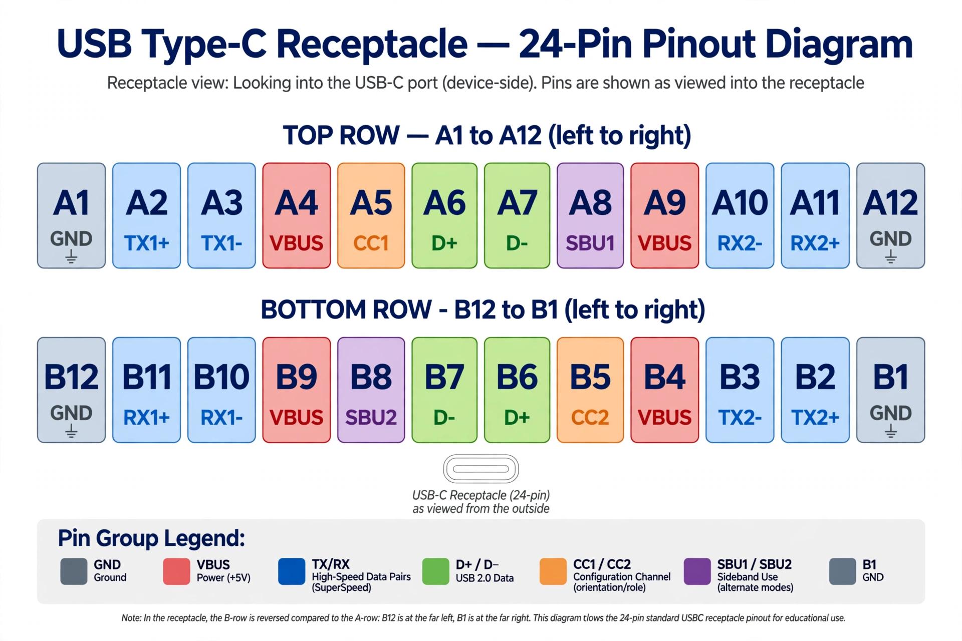
A professor's guide, from 20+ years on the bench, to laptop motherboard architecture and chip-level repair. We cover the USB-C 24-pin port, PD negotiation, and a real DX07BD24JJ2 board. This guide covers standard laptop PD only: 20V, 100W max.
Why Laptop Makers Left USB-A? The 6500x Speed Jump Story From My 20 Years Bench
In 1999 USB 1.1 gave us 12 Mbps and a connector you always inserted wrong. Today the same footprint delivers DisplayPort, PCIe Gen4 for Thunderbolt, 20V 100W power, and USB 2.0 simultaneously. Speed jumped from 12 Mbps to 40 Gbps — that is 6500x. Why did laptop makers leave USB-A? Single lane road vs 16-lane expressway. This section is pure bench memory, not datasheet copy.
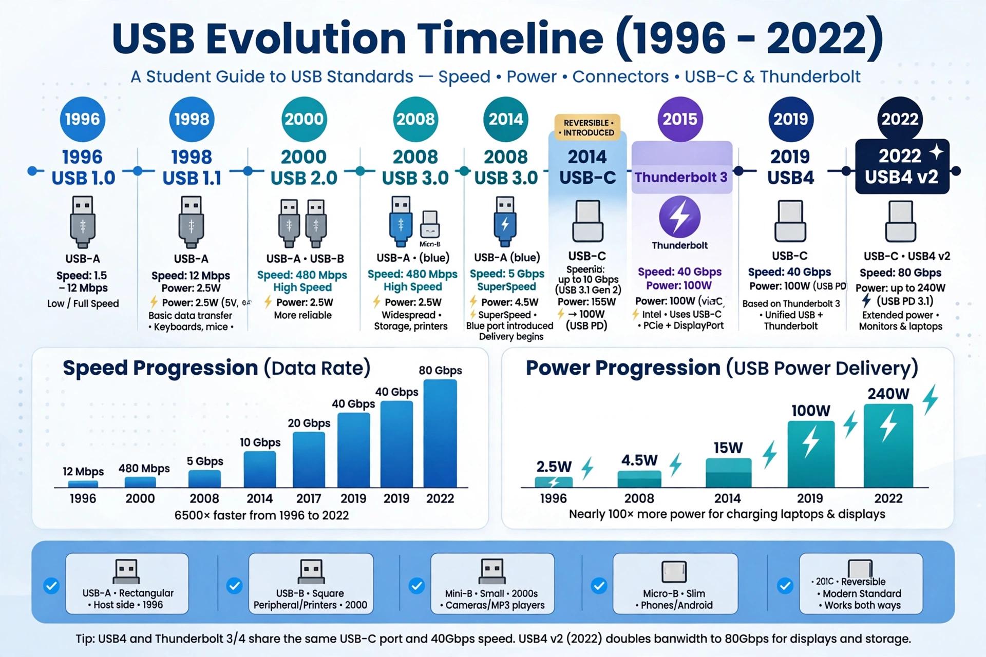
Professor's Tip: Think of USB evolution like road upgrades. USB 1.0 was a single-lane road (12 Mbps). USB-C is a 16-lane expressway with reversible lanes, smart traffic police (CC lines), and it can change from 5V low power to 20V 100W on demand. Same road, different rules managed by communication. No 48V here — laptop standard is 20V 100W MAX.
- 1999 Lab: USB 1.1 • 12 Mbps • 2.5W
- 2015 Shift: USB-C • 10Gbps • 20V 100W • Reversible
- 2026 Bench: TB4 • 40Gbps • 20V 100W MAX Laptop Standard
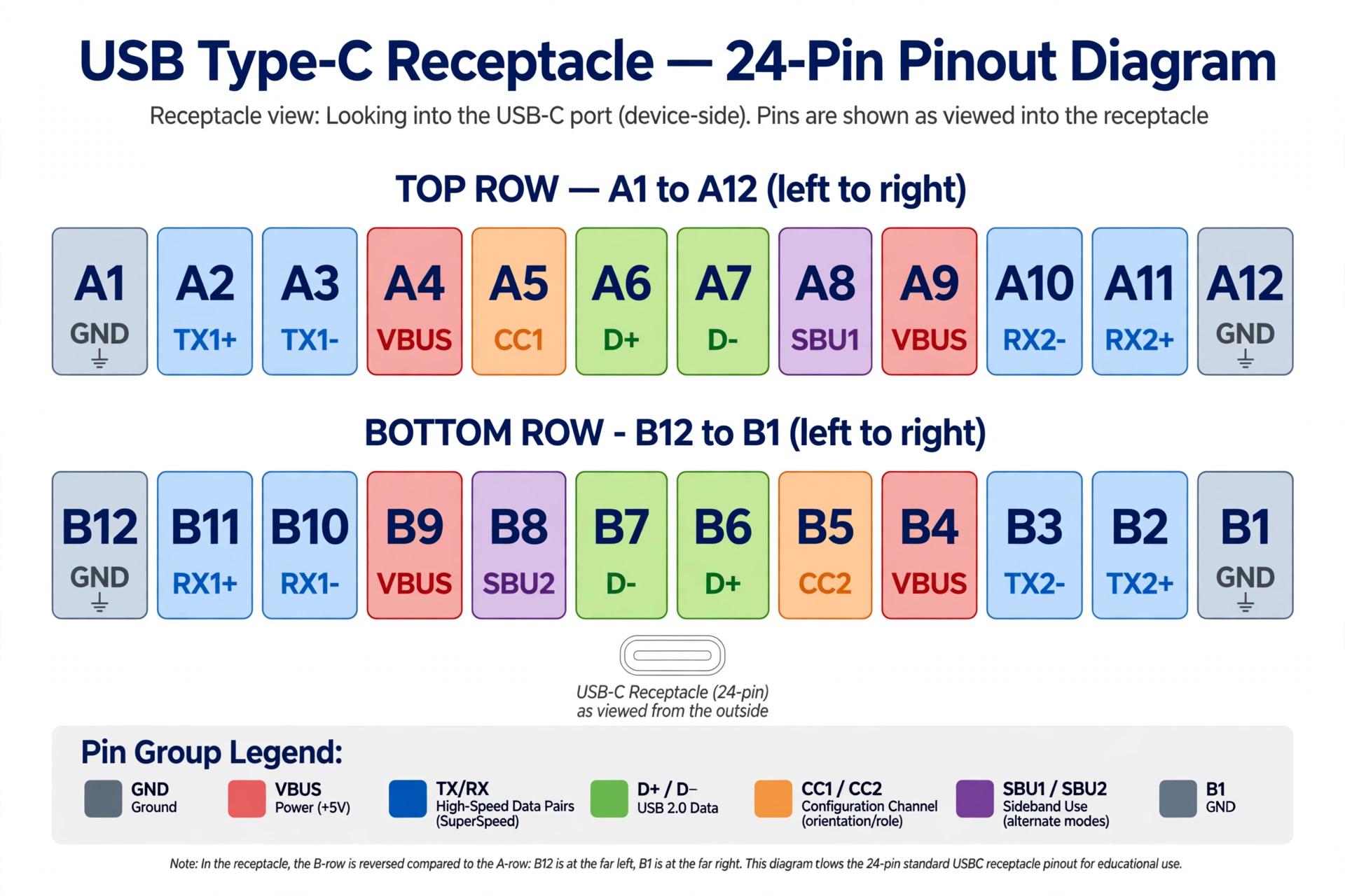
USB-C 24-Pin Truth: TOP/BOTTOM A1-A12 B1-B12 — VBUS, GND, TX/RX Explained
| Pin Group | Function | Typical Voltage |
|---|---|---|
| VBUS (A4, B4, A9, B9) | Main power. 4 pins parallel for current. Default 5V @ 900mA, after PD negotiation up to 20V 5A (100W MAX) for standard laptop PD. Laptop MAX is 20V 100W only. | 5V → 20V |
| GND (A1, B1, A12, B12) | Return. 4 pins parallel, low impedance. Measured to chassis should be <0.3Ω. Open GND = burning smell near connector. | 0V |
| CC1/CC2 (A5/B5) | Configuration Channel. Heart of USB-C. 300KHz BMC messages. Pull-down 5.1K = device present. Orientation + PD + Alt Mode detection. | 0.41V via 5.1K |
| D+/D- (A6, A7) | USB 2.0 legacy. 480Mbps. Still used for PD fallback, BIOS flash, slow devices. 90Ω differential. Protected by RT120/RT121 filters. | 0–3.3V |
| TX1+/-, RX1+/-, TX2+/-, RX2+/- | SuperSpeed. 10Gbps per pair, 20Gbps with 2 pairs, 40Gbps TB4. AC coupled with 0.22uF 6.3V caps. See the AC coupling section below for a deep dive. | AC coupled 0.22uF |
| SBU1/SBU2 (A8/B8) | Sideband Use. For Alt Mode: DP AUX channel. High impedance until alt mode. Goes to PS8740B mux. Short = no display but charge OK. | High-Z / AUX |
| VCONN (B5/A5 alt) | Power for eMarker IC in cable. 3.0–5.5V, 1W. Switched by PD controller when cable needs power. Not present in cheap cables. | 3.3–5V |
| Shield / Ground Springs | EMI & ESD. Must have low-impedance to board GND. Missing spring = display flicker on USB-C monitors. | Chassis 0V |
Voltage & Diode Reference — Wall Chart (20V 100W MAX Laptop Standard)
| Signal | Normal | Diode Mode (Red to GND) | Fault Means |
|---|---|---|---|
| VBUS | 0V no plug, 5V after attach, 20V after PD | 400–600 mV | 0 mV = shorted cap; OL = open trace |
| CC1/CC2 | 0.41V via 5.1K Rd | 450–700 mV via 5.1K path | OL = missing Rd resistor → no detection |
| D+/D- | 0V idle, 3.3V pulsing | 350–550 mV | Short to GND = USB2 dead |
| SBU1/2 | 0V or high-Z (~1.8V via PS8740B) | OL or 600–800 mV | 0–100mV = water damage short → no DP |
| TX/RX pairs | AC coupled → 0V DC | OL due to 0.22uF | 0Ω = short after cap, PS8740B/retimer fail |
Real Board Analysis: DX07BD24JJ2 LINK DONE Schematic — 0.22uF 6.3V, RT120 EMI Filter, SBU to PS8740B
Original sheet had correct topology but mixed labeling. Below is a cleaned, student-friendly decode. This is from a real laptop motherboard (Intel TB4 platform) with standard 20V 100W MAX PD design. No 48V EPR. Keep focus on 20V only.
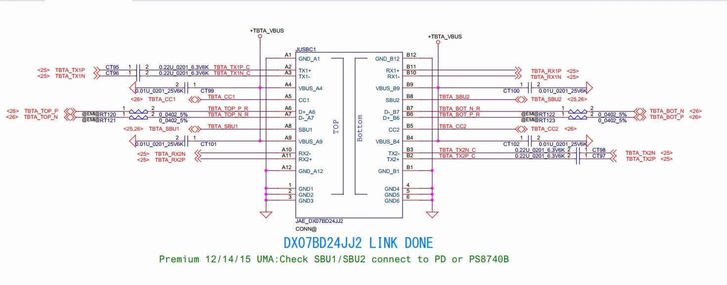
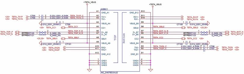
A) TBTA_TX1P_C / TBTA_TX1N_C — The 0.22uF 6.3V AC Coupling Caps
On the schematic, a 0.22uF 6.3V 0402 cap sits in series on TX1P/N and TX2P/N. SuperSpeed is AC coupled — DC is blocked to allow common-mode biasing. 0.22uF is chosen for 10Gbps: it passes high frequency and blocks DC. Diode mode shows OL because the cap blocks. If you read 0Ω after the cap → shorted retimer or PS8740B mux.
B) TBTA_CC1 — 0.01uF 25V Cap + 5.1K Rd Pull-Down
The CC line has a 0.01uF 25V cap to GND for filtering, plus a 5.1K resistor to GND (Rd). Purpose: kill RF noise so BMC 300KHz decoding is clean. If this cap shorts → CC stuck low → laptop never detects the plug. OL in diode mode means Rd is missing.
C) RT120 / RT121 — 0402 5% EMI Filters
These are D+/D- EMI filters, often a 90Ω common-mode choke + ESD combo. 0402 footprint, 5% tolerance. They protect USB2 from ESD and keep the eye clean. Fault: open = USB2 dead, but charging still works at 20V 100W if PD is OK.
D) SBU to PS8740B — The Hidden Link
SBU1/SBU2 go to the PS8740B MUX, not directly to the SoC. In Alt Mode DP, SBU carries AUX+ / AUX- (1Mbps bidirectional). If PS8740B fails, SBU shows short to GND → DP does not work but 20V charging does. PS8740B also handles orientation flip: it swaps SBU1/SBU2 based on CC orientation.
Debug trick: SBU short? Desolder PS8740B → short gone? → PS8740B is the culprit. Short remains? → trace or ESD diode near the JAE port.
Professor's Tip: When you see LINK DONE on a schematic, it means high-speed link training completed in that design revision. For repair, LINK DONE never means fault-free. Verify each AC cap, each Rd, each ESD diode. Standard is 20V 100W MAX, not 240W.
Why 0.22uF AC Coupling Is Mandatory? High-Speed Signal Postmortem on Real Schematic
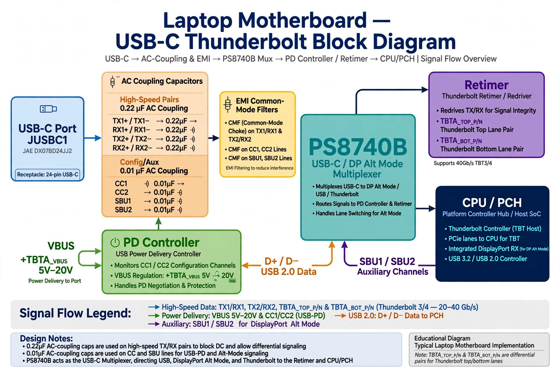
Why 0.22uF? High-speed differential pairs cannot tolerate DC bias mismatch between transmitter and receiver. The 0.22uF 6.3V 0402 acts as a DC block. It passes AC (10Gbps edge = 0.1ns) but blocks DC (0V average). Value calculated: for 10Gbps, a low-frequency cutoff of ~1MHz needs 0.1–0.22uF with 50Ω termination. Too large = slow charge, too small = baseline wander and eye collapse.
Postmortem Lab Check
- Measure diode on both sides of the 0.22uF: port side → OL (good); CPU side after mux → 400–600mV if an ESD diode is present, or OL if directly to the retimer
- If both sides show 0Ω → short after cap → PS8740B internal short or retimer
- Replace with the same part: 0.22uF 6.3V 0402 X5R, not a 10V or 25V MLCC with worse high-frequency response
Repair Bench Story (Real Case): Board with no USB3, only USB2 works. TX1P diode OL at the port side, but 12mV after the cap (short). Removed the 0.22uF, short remained on the CPU side → PS8740B short. Replaced PS8740B, USB3 back at 10Gbps. The 0.22uF cap was innocent, but it isolated the fault.
The Four Layers of the USB-C Path
- Layer 1 — Port: JAE DX07 receptacle → ESD TPD4E02 → AC caps 0.22uF → common-mode filters. First defense, first to fail.
- Layer 2 — Mux & Switch: PS8740B / HD3SS3212 flips TX/RX/SBU based on CC. Redriver boosts 6–12dB for long trace loss.
- Layer 3 — PD & Retimer: PD controller TPS65988 negotiates 20V 100W via BMC on CC. Retimer JHL8040 cleans jitter for 40Gbps TB4.
- Layer 4 — CPU / PCH: SoC xHCI + DDI (DP) + PCIe root. All converge. Fault here = no device in OS, but power still negotiates to 20V.
How 5V Becomes 20V? USB-C PD Negotiation Full Truth — 20V 100W MAX for Laptops
Default: every USB-C port outputs 5V with CC pulled low. When you plug in, the PD controller talks on CC using BMC 300KHz — digital negotiation. They exchange Source_Capabilities and Request. For laptops in this guide, standard PD max is 20V 5A = 100W MAX — no 48V EPR, no 240W. This is laptop standard, not phone EPR.
PD Contract Steps — Student Must Memorize (20V 100W Only)
- Attach detect — CC = ~0.41V via 5.1K Rd to GND = sink present
- Source advertises — 5V@3A, 9V@3A, 12V@3A, 15V@3A, 20V@5A
- Sink requests — Laptop EC requests 20V 100W via PD controller
- PS_RDY — VBUS rises from 5V to 20V in 275ms
- 100W MAX — 20V x 5A needs a 5A eMarker cable with VCONN
| Voltage | Power | Current | Note |
|---|---|---|---|
| 5V | 15W | 3A | Default |
| 9V | 27W | 3A | |
| 12V | 36W | 3A | |
| 15V | 45W | 3A | |
| 20V | 100W MAX | 5A | Laptop Standard |
Safety: Laptop PD max is 100W (20V x 5A). Higher voltages like 28V/36V/48V and 240W EPR are NOT used in this laptop design — this guide covers 20V 100W only. Laptian Technical Institute, Pune teaches the 20V standard for 12/14/15 UMA boards.
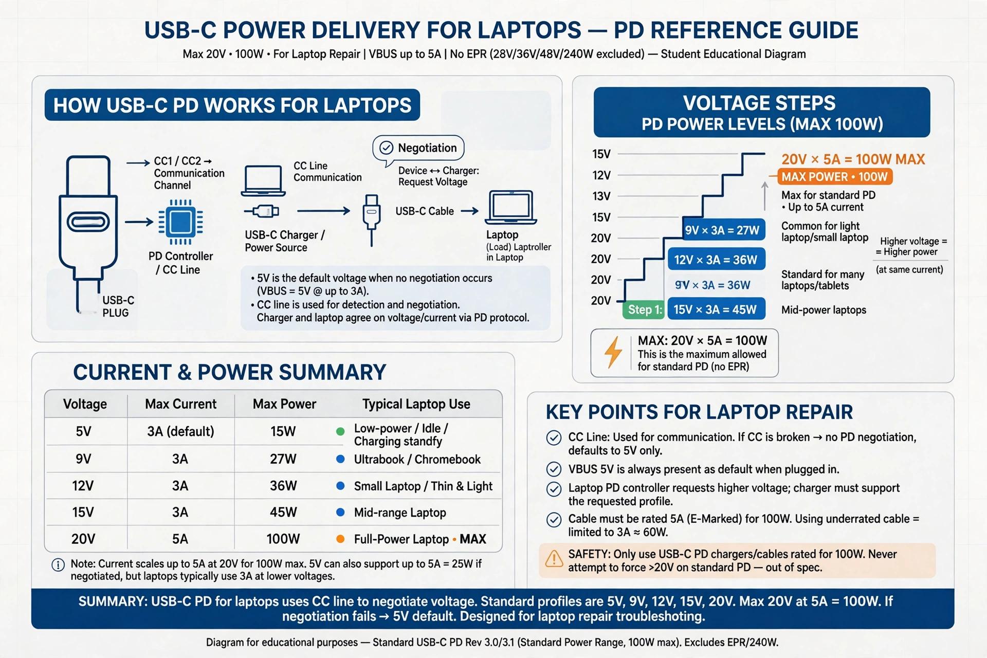
Professor's Tip: Never test 20V on VBUS with a multimeter directly while PD is negotiating — you will miss the transient. Use a PD trigger board. If VBUS stays 5V after plug, it is a PD controller or CC line fault, not the VBUS regulator. Laptop max here is 20V 100W.
SBU1 SBU2 Short = No Display? Premium 12/14/15 UMA Board Hidden Fault Exposed
Premium 12/14/15 UMA boards route SBU1/SBU2 from the JAE DX07BD24JJ2 to PS8740B, not the CPU. SBU carries DP AUX — 1Mbps bidirectional, critical for the display handshake. When SBU shorts to GND (water, dust), the laptop charges at 20V 100W but an external monitor shows no signal. Students check VBUS and CC only, and miss SBU.
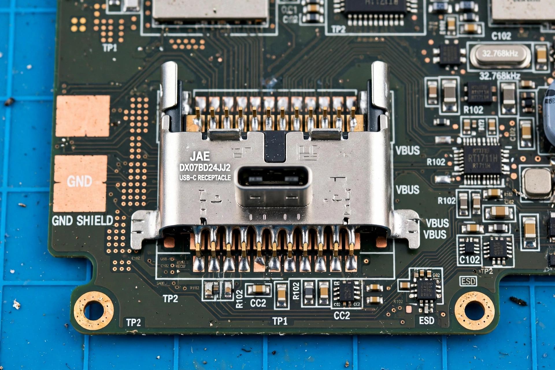
Why SBU Fault Is Hidden
- SBU traces are at the board edge, near the JAE, and corrode first
- Diode mode normal = OL or 600–800mV via PS8740B
- Fault diode = 0–100mV leakage to GND
- Charging is OK because VBUS and CC are a separate path
- PS8740B internal SBU switch fails short — common after liquid
Symptom: Type-C charging at 20V 100W works, but USB-C to HDMI/DP monitor shows no display, and the dock does not detect the display.
Fix: Clean with IPA, check ESD diode D12 near the JAE. Desolder PS8740B: if the short is gone, replace PS8740B. If it remains, trace corrosion.
Repair Bench Story (Real Case): 2023 case: ThinkPad T14 Gen2 — USB-C charged at 20V 100W, but no DP alt mode. VBUS diode 520mV normal, CC 480mV normal, SBU1 diode 18mV short. Cleaned the board, short remained. Desoldered PS8740B, short gone. Replaced PS8740B — display back. SBU fault is 20% of no-display cases on premium UMA boards.
5-Step Diagnosis: No 5.1K on CC Means No Charge — How to Check With Multimeter
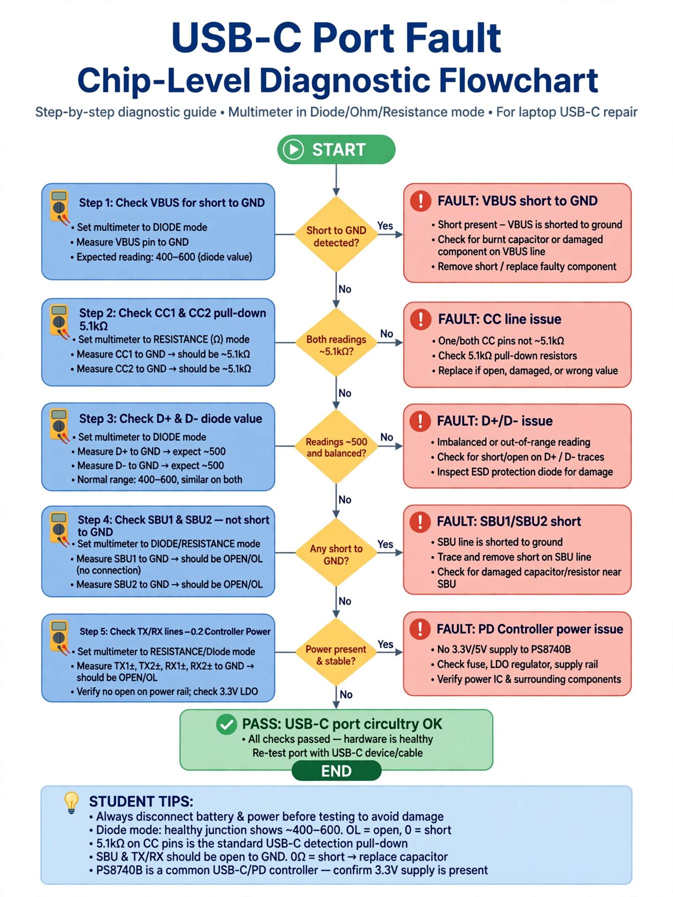
Step 1 — Visual & Power Off
Inspect the JAE DX07BD24JJ2 for bent pins and burn marks near VBUS A4/B4/A9/B9. Power OFF, disconnect the battery. Set the multimeter to diode mode, red probe to GND, black to the test point. A 10x magnifier is required. Tools: Magnifier 10x
Step 2 — VBUS Diode (Most Important)
Probe VBUS at the capacitor side, not the connector side. Good: 400–600mV. Short: <50mV. If short, inject 1V 1A via lab supply and feel for a hot cap with a thermal cam. Common culprit: a 10uF 25V MLCC cracked from board flex. Tools: Fluke 87V diode mode, thermal cam
Step 3 — CC1/CC2 5.1K Check
CC must be 450–700mV due to the 5.1K Rd to GND. If OL → Rd resistor open or trace cut after a drop. If 0mV → CC filter cap 0.01uF shorted. Remove the cap to confirm. No 5.1K = no charge detection, even if VBUS is good. This is the key fault for a dead port. Tools: measure at RT120 near the JAE
Step 4 — D+/D- USB2 EMI Filter
350–550mV is normal. If short to GND, check the RT120/RT121 EMI filter (0402, 5%). Desolder the filter and re-measure. If still short → ESD IC TPD4E02 or CPU side. USB2 may be dead while 20V charging still works. Tools: Hot air 350°C
Step 5 — SBU1/SBU2 & TX/RX Final
SBU: OL or 600–800mV is OK. 0–100mV → water damage short → no display. TX/RX: OL is expected due to the 0.22uF AC cap blocking DC. If 0Ω → short after cap: suspect PS8740B or retimer JHL8040. Power-on check: CC should rise to ~0.41V with a charger, plus BMC pulsing on the scope. No pulsing → PD controller TPS65988 not responding. Check its 3.3V LDO and I2C. Tools: Oscilloscope 100MHz; check both sides of the 0.22uF
Repair Bench Story (Real Case): One board: VBUS diode 12mV, dead short. Injected 1V, C32 near the JAE got hot in 2 seconds. It was a 10uF 25V VBUS bulk cap cracked due to board flex. Replaced with the same value, 25V X5R. Diode returned to 520mV. Saved a Rs. 18k motherboard. Always use thermal, not guessing. Laptian Technical Institute, Pune trains this method.
Comparison — USB-A vs USB-C vs Thunderbolt 4 (20V 100W Standard Only)
| Feature | USB-A | USB-C (USB3.2) | Thunderbolt 4 (USB-C form) |
|---|---|---|---|
| Pins | 4 | 24 | 24 (same) |
| Reversible | No | Yes (CC detect via 5.1K) | Yes |
| Speed | 480Mbps | 10Gbps (1 pair), 20Gbps (2 pairs) | 40Gbps PCIe + DP |
| Power | 5V 0.5A (2.5W) | 5–20V up to 100W MAX Standard PD | Up to 100W + 15W bus power |
| Alt Mode | No | Yes: DP, HDMI | Mandatory DP, PCIe mandatory |
| Cable IC | None | eMarker for >3A | Active retimers + eMarker |
| Typical Fault | Broken tongue | VBUS cap short, CC 5.1K open | Retimer fail, SBU short no display |
Student FAQ — 3 Most Asked Lab Questions (20V 100W Verified)
- Why 0.22uF cap on TX/RX?
- The 0.22uF 6.3V 0402 cap on TX/RX is AC coupling. SuperSpeed signals are AC coupled to block DC and allow common-mode biasing at both ends. 0.22uF passes 10Gbps high-frequency while blocking DC. Too large slows the edge, too small causes eye diagram failure. In diode mode it shows OL normally because the cap blocks DC; 0 ohm means short after cap — check PS8740B or retimer JHL8040. Always replace with the same value X5R, not random.
- Why CC needs 5.1K?
- CC needs a 5.1K Rd pull-down to GND for sink detection. When a device plugs in, the source detects approximately 0.41V on CC via this resistor, confirming attachment and orientation (CC1 vs CC2). Without 5.1K, the laptop never detects the charger — dead port even if VBUS caps are good. Diode mode should show 450–700mV via the 5.1K path; OL means an open resistor near the JAE, common after a drop or liquid. Also check the 0.01uF filter cap for short.
- Why SBU short causes no display?
- SBU1/SBU2 carry the DisplayPort AUX channel in Alt Mode (1Mbps bidirectional). They go to the PS8740B mux, not directly to the CPU. If SBU shorts to GND due to water damage or a failed PS8740B, the AUX handshake fails, so the external display shows no image while 20V 100W charging still works. Check diode: OL or 600–800mV is normal, 0–100mV indicates a corrosion short. Fix: clean with IPA, check the ESD diode near the JAE, desolder PS8740B to isolate.
Student Lab Checklist — Before Touching the Board (20V 100W Only)
- Print the pinout diagram and voltage table, stick them on the wall
- Always diode mode first, power OFF, battery out
- VBUS short? Use 1V 2A injection + thermal cam, not 20V
- CC OL? Check the 5.1K Rd resistor near the JAE, not the CPU
- SBU short? Suspect water → clean, check ESD diode first
- TX/RX OL is NORMAL (0.22uF blocking), 0Ω is a fault
- After repair, test with 3 cables: charge-only, 10G data, DP alt mode
- Log diode values: VBUS 400–600, CC 450–700, D+/D- 350–550
Want to practise this on live motherboards? Explore chip-level laptop repair training at Laptian Technical Institute, Pune.
Note: All schematics are JAE DX07BD24JJ2 real board examples, shared as educational fair use. Diode values are typical and vary by board. Always refer to the boardview. Laptop PD max is 20V 100W, no 48V/240W in this design.